Salah Bedair

Biography
Dr. Bedair currently investigates semi-conductor materials and devices including novel growth techniques such as atomic layer epitaxy, laser-assisted diposition, molecular beam epitexy and chemical vapor diposition. He also studies optical, electrical and structural properties of semiconductors, epitaxial insulators and quantum well structures. Optical and microwave devices such as detectors, wave guides, solar cells, light emitting diodes, semiconductor light bulbs and modulation doped field effect transistors are currently considered in Dr. Bedair's lab.
Education
-
Ph.D.
1969
Engineering Science
University of California, Berkley -
Master's
1965
Nuclear Engineering
University of California, Berkley -
Bachelor's
1960
Electrical Engineering
Alexandria University, Egypt
Highlighted Awards
Awards & Honors
- 2015 - Alexander Quarles Holladay Medal for Excellence (NC State)
- 1998 - Alumni Association Distinguished Graduate Professorship (NC State)
- 1992 - IEEE Fellow, Contribution to Atomic Layer Epitaxy
- 1992 - R J Reynolds for Excellence in Teaching, Research and Extension (NC State)
- 1988 - ALCOA Foundation Distinguished Engineering Research Award (NC State)
- 1986 - Department of Energy Award (Development of Cascade Solar Cells)
Recent News

Optimizing InGaN templates for LEDs
Posted on March 15, 2022 | Filed Under: News and Quantum
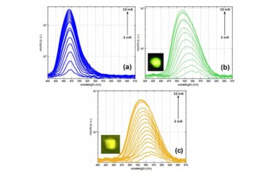
North Carolina State University has been investigating the potential of indium gallium nitride (InGaN) for enhancing the performance of III-nitride light-emitting diodes (LEDs)

New Synthesis Process Paves Way for More Efficient Lasers, LEDs
Posted on October 27, 2021 | Filed Under: Quantum and Research
A new process uses existing techniques to make more efficient LEDs and lasers.
Dr. Salah Bedair Awarded Holladay Medal
Posted on April 16, 2015 | Filed Under: News
Five professors received the Alexander Quarles Holladay Medal for Excellence, including Salah M. Bedair, professor of electrical and computer engineering.
Media Mentions

New Connection Between Stacked Solar Cells Can Handle Energy Of 70,000 Suns
September 16, 2013
NC State researchers have come up with a new technique for improving the connections between stacked solar cells, which should improve the overall efficiency of solar energy devices and reduce the cost of solar energy production. Salah Bedair, electrical engineering, featured.

New Method Improves Solar Energy Efficiency, Cuts Costs
September 10, 2013
NC State researchers have developed a simple fix to increase the efficiency of stacked solar cells dramatically. Salah Bedair, electrical engineering, featured.

How to Harness the Power of 70,000 Suns
September 9, 2013
NC State researchers have come up with a new technique that which should improve the overall efficiency of solar energy devices and reduce the cost of solar energy production. Salah Bedair, electrical engineering, featured.
